
TL;DR

Get business pricing on garage and car supplies
- Business-only prices and quantity discounts
- Tax-exempt purchasing
- Multiple users, one account, clear invoices
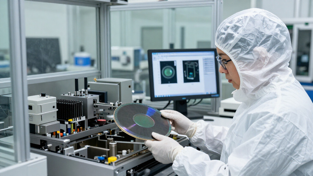
Infineon says it has made functional power devices from 300 mm silicon carbide wafers at its Villach, Austria, fab using existing silicon manufacturing equipment. The company calls this a milestone toward possible industrial-scale production, but has not announced a customer ramp schedule; it will plan technology and timing with customers and partners while continuing its 200 mm SiC roadmap.
Infineon Technologies says it has processed 300 mm silicon carbide (SiC) wafers into functional power devices at its Villach, Austria, fab, using existing silicon manufacturing equipment. The company describes the work as a milestone toward manufacturing SiC at larger scale; it has not announced when commercial production on 300 mm wafers could begin.
The devices were made in a full-scale semiconductor fab environment, rather than only in a laboratory process, according to Infineon. The company says it is the first to reach this milestone in such an environment. That priority claim comes from Infineon; the supplied report does not cite an independent assessment or name the devices produced, their performance, or whether customers have tested them.
Infineon says a 300 mm wafer can yield 2.3 times as many chips as a 200 mm wafer. That is a potential wafer-area and output advantage, not a reported increase in production volume or a measure of cost savings. The company has not provided yield figures, device volumes, manufacturing costs, or details on how much of its existing equipment can be used without modification.
The company also reported demonstrating its Cold Split technology on 300 mm SiC at its Dresden site. The process separates wafers from a silicon carbide boule. Infineon says Cold Split reduces material loss and processing time compared with conventional wire sawing, allowing more wafers to be obtained from the same crystal with less capital expenditure. The report does not include measured comparisons or production data for the process.
A Larger Wafer Route for Power Devices
If the process can be developed into reliable, high-volume manufacturing, larger wafers could let producers make more devices from each wafer and use established silicon fab infrastructure. Infineon’s reported use of existing equipment is relevant because it points to a possible way to expand SiC processing without building an entirely separate production environment. The company has not disclosed what investment would be required to convert that possibility into commercial output.
SiC power devices are used where efficient control and conversion of electrical power matter. Infineon says its CoolSiC portfolio serves traction inverters and on-board chargers in electric vehicles, EV charging equipment, large-scale energy storage, industrial drives and uninterruptible power supplies. The company also lists solid-state transformers, circuit breakers and power supply units for AI data centers. The announcement concerns manufacturing capability; it does not establish that devices for these applications are already being made at commercial scale on 300 mm wafers.
The development is also relevant to the supply chain for power semiconductors, where manufacturers are working across silicon, SiC and gallium nitride technologies. A larger-wafer process could affect future capacity and production economics, but the announcement provides no forecast for prices, output, customer supply, or the timing of any such effects.
Products Worth Considering

DEWALT 20V MAX 9-Tool Combo Kit with Impact Driver, Drill Driver, Oscillating Tool, Grinder, Circular Saw, Reciprocating Saw, Right Angle Dr

DEWALT 20V MAX XR Hammer Drill and Impact Driver Combo Kit with Two 4Ah Batteries and Charger

Chemical Guys 10-Piece Car Wash Kit with Foam Gun
As an affiliate, we earn on qualifying purchases.
Infineon’s SiC and Wafer Plans
Infineon says it will continue its 200 mm SiC roadmap while planning the technology and timing for 300 mm SiC with customers and partners. That makes the new result a development alongside its existing roadmap, not an announcement that current production is moving to the larger wafer size.
The company’s report also cites its work on other wafer formats and power materials. On October 27, Infineon announced an investment of about €1.1 billion in a high-volume facility for gallium nitride (GaN) power semiconductors on 300 mm wafers in Villach. GaN is a different semiconductor material from SiC, and the investment announcement does not confirm that the new SiC process will use the same facility or schedule.
The latest SiC milestone links two reported steps: processing 300 mm wafers into functional devices at Villach and demonstrating a wafer-separation method at Dresden. Together, they indicate progress on both device processing and wafer preparation, but the company has not said that the two steps have been combined into a qualified, volume-ready production flow.
“This technological milestone further strengthens our leadership in power systems.”
— Jochen Hanebeck, CEO of Infineon Technologies
Commercial Scale Still Undetermined
Infineon has not published a commercial production start date, a ramp schedule, or expected output for 300 mm SiC. It says planning will take place with customers and partners, but has not identified those partners or disclosed customer commitments.
Other unanswered questions include the devices’ measured performance, manufacturing yields, qualification status, process costs and the changes, if any, needed to adapt silicon equipment for SiC. The company’s claim that it is first to achieve the milestone in a full-scale fab is not independently substantiated in the supplied report. Nor are comparative data provided for the material savings and processing time attributed to Cold Split.
Customer Planning Sets the Timeline
Infineon says it will work with customers and partners to plan the 300 mm SiC technology and determine a ramp schedule. The company has not given a date for those plans or named a next public milestone. Until further details are released, the result should be read as a manufacturing milestone rather than confirmation of volume production.
Readers can look for updates on qualification, device types, yields, investment requirements and customer adoption. Infineon also says it will continue its 200 mm SiC roadmap, so developments on that track remain relevant while the company evaluates the larger-wafer process.
Key Questions
What did Infineon report?
Infineon says it processed 300 mm SiC wafers into functional power devices at its Villach, Austria, fab, using existing silicon manufacturing equipment.
Does this mean 300 mm SiC devices are in mass production?
No. The announcement describes a manufacturing milestone, but Infineon has not announced a commercial production date, volume, or ramp schedule.
What is the reported wafer-yield advantage?
Infineon says a 300 mm wafer yields 2.3 times as many chips as a 200 mm wafer. The company has not published production yield or cost figures for its new process.
What is Cold Split?
It is Infineon’s method for separating wafers from a SiC boule. The company says it causes less material loss and takes less processing time than conventional wire sawing, but the announcement provides no measured comparison.
What happens to Infineon’s 200 mm SiC plans?
Infineon says it will continue its 200 mm SiC roadmap while planning the 300 mm technology and timing with customers and partners.
Source: chargedevs.com